
glossary
Wafer
Wafer is a thin, round slice of crystal that a factory paints, cuts, and fills until many copies sit on one disk.
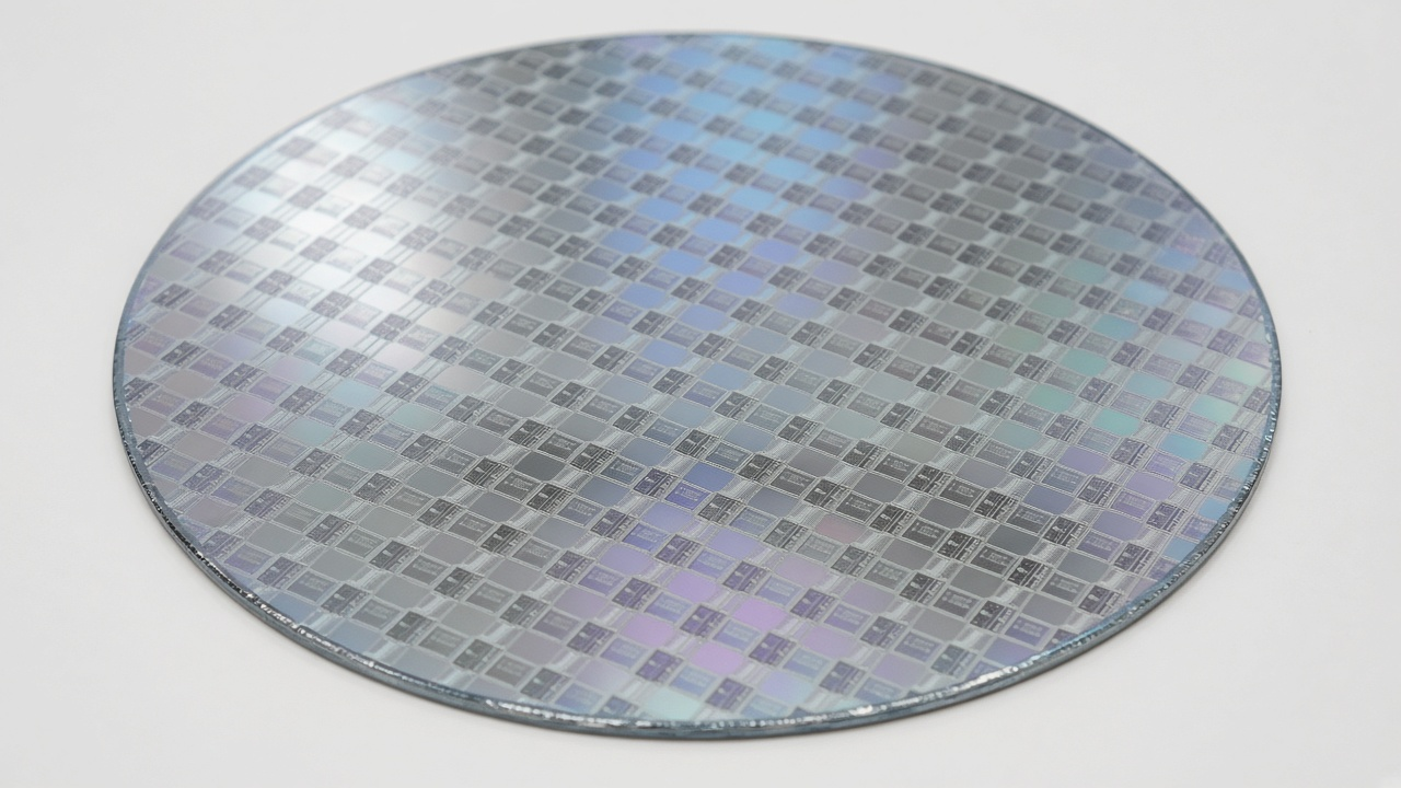
A round disk carrying many copies of the circuit.
The drawing is printed many times across that disk. Yield, cost, and some rules (density, fill, and edge exclusion) are wafer stories. A 300 millimeter wafer can hold hundreds of copies of a 10 millimeter die. A student MEMS run might use 100 millimeters. The drawing still looks like one chip. The economics are per wafer. In the factory the object is a mirror-like disk in a cassette, or a map of repeated fields with a flat or notch for orientation. Streets between copies are the scribe lines where a saw or laser will cut.
The image that prints each field comes from a photomask or a reticle on a stepper, unless an e-beam writes the wafer directly. After processing, each cut-out chip is a die. The editor’s square outline is usually one die, or one reticle field. The wafer is the round thing in the factory.
Edge exclusion is a ring, often 2 or 3 millimeters, where dies are not trusted. A wafer map shows a gray halo, and the yield number ignores that halo. Fill and density rules still apply near the edge. A multi-project wafer shares one reticle among many dies. The scribe must match the shuttle, not a private wish.
The plate, the camera, and the recipe are covered in what a photomask is, steppers and why size matters, and MEMS is layout plus a recipe.