
Masks · Fab
Steppers and why size matters
The machine prints a field, then steps. Your die has to fit that window, not only the wafer.

You are printing many copies of a chip onto a round wafer, one rectangle at a time. The machine that does the printing is a stepper, or a scanner that sweeps instead of flashing. The glass it holds is a reticle. The lens usually shrinks. Your die has to fit the window that lens can print, not only the wafer. Grow the die by a millimeter and you can lose a whole ring of sites, not one percent of area.
The picture at the top is a wafer after that walk. Rectangular fields tile the disc. Where the rectangle meets the round edge, the field is cut off. Those partial sites are not a drawing error. They are the rim of a circle that refused to become a square.
A field, then a step
A wafer is large. A lens field is not. A layout that is “smaller than the wafer” can still be too big for one shot. The machine prints a field, steps the chuck to the next site, and prints again. If your chip is wider than the field, the tool will not crop politely. It will refuse, clip, or demand a split you did not design.
A common 4× reduction scanner prints a field up to about 26 mm by 33 mm on the wafer. That number is the rectangle on scanner data sheets. Older steppers often reduced 5× and offered a smaller window. A contact aligner, by contrast, prints 1:1 and can cover a much larger piece of the wafer in one flash, because there is no reduction lens in the way. The photograph below puts the two sizes in one frame: the glass plate carries a large pattern, and the wafer beside it carries a much smaller print of the same idea.

On a 4× lens, chrome is four times the wafer size. A 5 mm die is 20 mm of pattern on the glass, plus alignment marks and a frame. A field of 26 mm by 33 mm can hold several such dice. That cluster is drawn on the reticle. It is not the same thing as an array of cells inside the file. An array in the editor is hierarchy. A step on the tool is the chuck moving. You may draw one die and let the machine repeat it across the wafer. You may also draw a 2 by 2 of dice so one flash fills the field. Name which repetition you mean on the order.
People care about die size because of this window, and because of how many good dice fit on the round wafer after the edge fields are lost. A die that grew past the field does not cost a little more silicon. It may not print on the tool you hired.
What the scanner changes
A scanner does not flash the whole field at once. A slit of light crosses the wafer while the reticle and the wafer move together, the wafer slower by the reduction factor. The picture below is that slit: a narrow band of light on a round wafer, inside the tool. For the person drawing the chip, the slit is still a field with a maximum rectangle. The chuck still steps to the next site when the slit has finished its pass.

Where the size goes wrong
A die plus the saw lane can be larger than the field. A 21 mm die in a 22 mm window can fail once you add the scribe on both sides. Count the frame, not only the circuit.
The purchase order has to name the shrink, 4× or 5× or 1:1. If you enlarge the layout 4× “to help the mask shop” and they also enlarge 4×, the wafer sees 16×. If you draw at wafer scale and they write 1:1 glass for a 4× camera, every feature arrives four times too large. Measure a known bar on the first wafers.
Alignment marks have to be on a layer that becomes chrome. The camera cannot find a mark that was only a color on your screen.
The file does not have to contain the stepper’s walk. The file can be one die. The machine is allowed to repeat it across the wafer. Say so, or the shop may print one lonely field and call the order complete.
How many dice the circle allows
Look again at the wafer at the top. The fields are a grid. The wafer is a disc. Every field that hangs off the rim is a partial exposure: some dice in that field never become chips, and the saw cannot invent the missing silicon. A die that is 10 mm on a side with a 100 µm scribe does not yield “wafer area divided by die area.” It yields the number of full rectangles that sit inside the circle, after the field size and the scribe have taken their cut.
On a wafer map from the foundry, or on that picture, count the fields the rim has cut and the fields that are complete. Multiply the complete fields by the number of dice you placed on one reticle. That product is how many chips this wafer can give you. If a one-millimeter growth of the die drops a row of those complete fields, the area formula will not show the loss. The ring is gone, and the count is the only place you will see it.
If you are sending the plate to a university stepper, read that tool’s field and its shrink before you freeze the die. A 26 mm by 33 mm scanner field and a 15 mm teaching-stepper field are different rooms. The same GDS can be legal in one and impossible in the other, with every polygon still on grid.
Continue exploring
-
 What is a photomask? The glass plate that prints a chip
A photomask, also called a reticle, is a quartz plate with a chrome pattern. Light shines through it to copy one layer of a chip onto a wafer, and a chip needs a stack of them.
-
 Cell arrays and step-and-repeat: rows, columns, pitch, and AREF
An array places one cell in rows and columns at a fixed pitch and is stored as one array reference (AREF in GDSII). How a wrong step adds up across the grid, and why one record has one rotation.
-
 The drawing is not the thing you build
Glass, silicon, and fiberglass are different objects that can share one geometry.
-
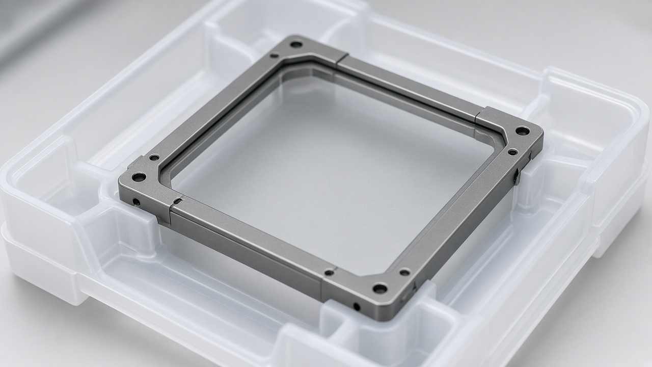 Reticle
-
 From idea to something a shop can print
How a napkin sketch becomes a file, a cover letter, and a glass plate a shop can print from.