
glossary
Die
A die (plural dice or dies) is one finished rectangle cut from the disk: the part that was designed, plus whatever streets the saw needed.
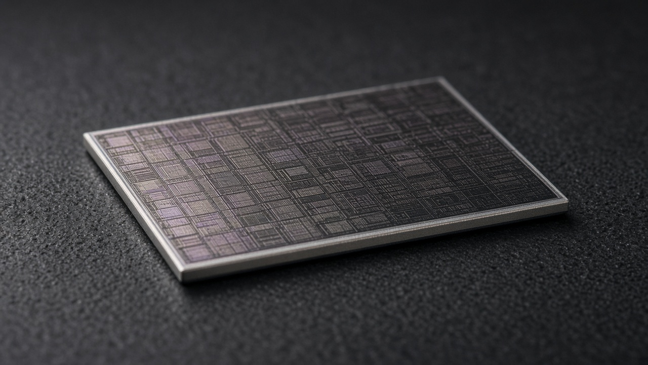
One rectangle cut from the disk. The rest of the wafer is not in the picture.
Area is money. A die that grows 10 percent can drop the number of good copies on a wafer by more than 10 percent after streets and edge loss. Pads, seal rings, and alignment marks live at the die edge. The useful circuit lives inside. In the file the die is the top cell outline, perhaps 2 millimeters by 2 millimeters for a small analog part, or 15 millimeters on a side for a large processor. After sawing, the die is the piece that goes into a package. The gaps between dies on the wafer are scribe streets. A reticle field may hold one die or several. The file you edit is usually one die, not the whole wafer map. The packaged part is a different object. The package is the plastic or ceramic house. The die is the silicon, or glass, or other substrate inside.
Packaging cares about die size too. A 5 by 5 millimeter die in a 5 by 5 millimeter package is a prayer. Bond pads may sit on an 80 micrometer pitch along the edge, or a bump array may sit on a 150 micrometer pitch for flip-chip. The scribe is outside the die. Do not park a seal ring in the street. The top cell outline should match the foundry’s die photo.
What that rectangle is inside a layout, what a photomask does with it, and why the field size matters are covered in what is a layout, what a photomask is, and steppers and why size matters.