
glossary
MEMS
MEMS (micro-electromechanical systems) is the field of tiny moving or sensing parts built with the same kind of drawings as chips, plus a factory recipe that cuts, grows, and frees them.
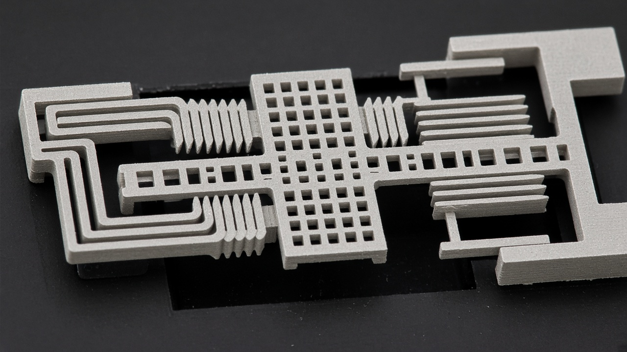
A tiny structure that can move, built with the same kind of drawing as a chip.
The file looks familiar. It still holds a layer, a cell, and a polygon. The failure is new. A beam 2 micrometers thick and 100 micrometers long is a spring. A missing release hole is a brick. Voltage, squeeze-film air, and stress matter as much as width. On screen the part is a comb drive, a membrane with a grid of holes, or a mirror on torsion springs. The editor still shows 2-D colors. The object is a 3-D machine.
The recipe includes photoresist, deposit, and etch. A cousin that pushes liquid rather than a solid part is microfluidic work. Electronics on the same die still need DRC and often LVS. Sending a MEMS GDS to a CMOS mask shop and hoping leaves the recipe behind. The layer map and the release chemistry are the product. Geometry without the recipe is a picture.
Ask for the cross-section before the 2-D art is finished. A 2 micrometer structural film over a 3 micrometer sacrificial film is a different spring than the inverse. Dimples are drawn to fight stiction, and anchors are sized for enclosure after the release etch. Treat the recipe document as a sibling of the stream, not as optional reading. The drawing plus that recipe is MEMS is layout plus a recipe. The sheets underneath are still what is a layout. The cut that shows which film is which is looking at a cross section.