
glossary
Deposit
A deposit (deposition) is a process step that adds a film — grow, sputter, plate, or coat — so the disk gets thicker in a controlled way.
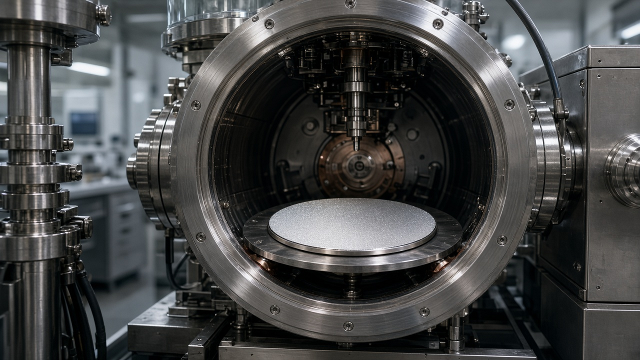
A chamber that adds a film onto a disk.
The stack is built, not carved from a solid block. Oxide, nitride, metal, poly, and polymers each arrive with a thickness and a way they cover steps. A 0.5 micrometer oxide on a 2 micrometer trench does not look like the cartoon rectangle in the editor. In a cross-section the new film is a band on top of the last band. In the file you still draw a 2-D layer. The recipe says 300 nanometers. The drawing says where. Deposit pairs with etch. Patterned photoresist can lift off a deposit, so material stays where the resist was not, or the resist can survive while a film is etched. A release later removes a sacrificial deposit under a moving part. Treating every layer as paint on a flat table ignores coverage, seams, and stress, which is why MEMS people talk about recipes as much as about polygons.
Conformal films coat sidewalls. Sputtered films shade steps. A 0.3 micrometer nitride can look continuous in the cartoon and thin on a sharp corner in the SEM. Layout still owns the 2-D opening that lets the film in or keeps it out. A release hole pattern is a deposit-and-etch conversation, not a decoration layer.
How the recipe and the drawing share the job, what a cross-section shows, and what that sheet is for are covered in MEMS is layout plus a recipe, looking at a cross section, and what a layer is for.