
glossary
Photoresist
Photoresist (resist) is a light-sensitive film coated on the disk, exposed through a plate or with a beam, then developed so some of it stays as a stencil.
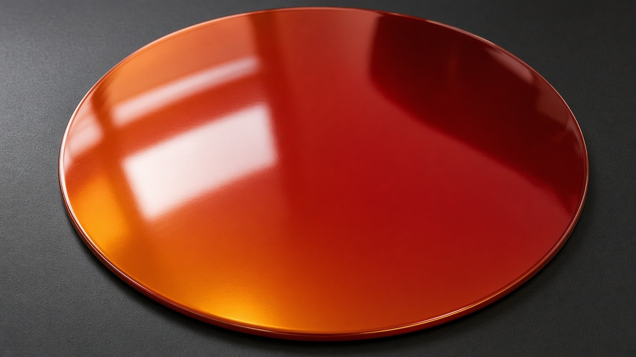
A shiny unbroken coat on the disk, waiting to be exposed.
Almost every printed step starts as that film. Light through a photomask, or an e-beam writing directly, turns it into a stencil for etch or deposit. Positive resist leaves material where it was dark. Negative resist does the opposite. The layer polarity has to match the process, not a preference for dark or light on screen. In a lab the coat looks golden or reddish, then a pattern after develop. A 1 micrometer line in resist is the stencil. The metal or the hole comes next.
On a MEMS run a thick resist can be the mold itself. On a chip line, resist is usually sacrificial. Thickness is a knob. A 0.5 micrometer resist for a fine gate is not the 10 micrometer resist a MEMS mold uses. Standing-wave ripples show up on reflective metal when the stack is wrong. The drawing still owns the two-dimensional opening. The process owns bake, dose, and develop. The colorful layout is an instruction, not the resist. If the process inverts polarity, a dark drawing becomes a hole, not a wall. Write that polarity in the layer map so a dark drawing does not become an unwanted etch.
See what a photomask is, MEMS is layout plus a recipe, and what is a layout.