
glossary
Photomask
A photomask is a glass plate with a patterned film that casts a shadow, so light can print a drawing onto a round crystal disk.
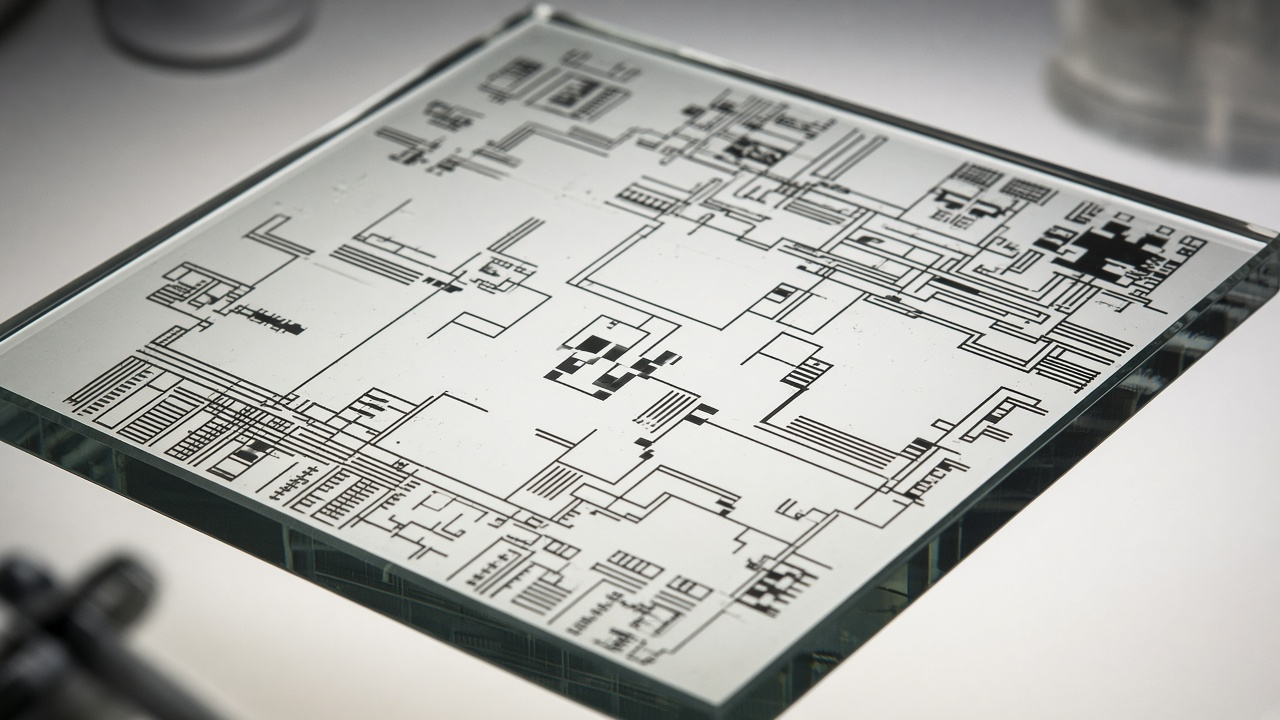
A glass plate with a dark pattern. Light through that pattern is how the drawing is printed.
Most chip factories do not write rectangles one by one. They shine light through a mask, or reflect it from one, and print a field. If a shape is wrong on the mask, every printed copy is wrong. The drawing in the editor is a letter to the mask shop: which layer becomes chrome, which polarity, and which scale. The object in the box is a quartz plate, or a picture of dark features on a clear field. A 0.25 micrometer gate on the wafer may be four times larger on a 4× mask, depending on the stepper.
A reticle is the usual name when the plate holds one or a few chip fields for a stepper, not a 1:1 contact print of a whole wafer. Writing without a plate, shape by shape, is e-beam lithography. The colorful editor view is a stack of drawing layers. The mask is one sheet and one polarity, after fracture and often after OPC. That stack is many future plates, plus notes that must never become chrome. How one plate is made from one sheet is what a photomask is. The drawing those sheets come from is what is a layout. The camera that prints a field and steps is steppers and why size matters.