
Masks · Fab · Hierarchy
Reticle layout versus wafer layout
A reticle layout is the cell the mask shop writes; a wafer layout is the stepper job that places its images on the wafer. LayoutEditor rule files check the reticle cell against the exposure field and count dice on a simulated wafer.
Last edited: November 12, 2026

A reticle layout is the cell that a mask shop writes onto a stepper reticle: one or more images, each a rectangular pattern that the stepper can expose on its own. A wafer layout is the placement of those exposures on the wafer: which image is exposed at which position, on which step pitch, and for which process layer. On a projection stepper the two are separate data. The reticle layout is mask data in a GDSII or OASIS file. The wafer layout is a program in the stepper job and is never written on any plate. The repeating unit inside an image is the die cell, the future chip including its seal ring. Mask data preparation places that die several times as a matrix on the final reticle, separated by horizontal and vertical scribe lines, and the maximum reticle field of the exposure tool limits the size of the matrix (Lienig and Scheible, Fundamentals of Layout Design for Electronic Circuits, 2020, ch. 3.3).
The picture at the top is a LayoutEditor view of a simulated wafer layout. The black circle is a 100 mm wafer, the orange circle the usable area with a 3 mm edge clearance. Each navy square is one shot of a 10.000 mm image that holds 2 × 2 dice of 4.900 mm. The 240 dice filled in green lie completely inside the usable area; LayoutEditor counted them with the rule file in the section on counting dice below. The white dice lie in exposed shots but cross the edge of the usable area or of the wafer.
Three cells, three consumers
The UCSB Nanofab stepper guidelines recommend a cell named reticle_layout as "an exact representation" of the printed reticle patterns, typically at 1x wafer scale, with the device cells instanced into it; the same device cells can also be instanced into device_layout and wafer_layout cells for design and verification. The reticle_layout cell is the one named on the mask order.
| Cell | Contents | Scale in the file | Used by |
|---|---|---|---|
DIE |
one chip: circuit, pads, seal ring | 1x wafer scale | DRC, LVS, the designer |
RETICLE_LAYOUT |
every image at its position on the plate, chrome between the images | 1x wafer scale; the shop writes it 4x or 5x larger | mask shop (top cell on the order form) |
WAFER_LAYOUT |
shots of the images across a drawn wafer | 1x wafer scale | the designer, to plan the stepper job; not sent to the shop |
The three names are conventions, not records in the file. A GDSII file has no record that marks a top cell, so the order form names it; see naming the top cell you ship. The repetition inside an image is an array reference in the file; the repetition across the wafer is stage movement. Arrays and step and repeat describes the file record.
What the reticle cell holds
An image is a region of the reticle that the stepper's shutter blades can isolate. The blades open a window of the image size and block the rest of the plate. The chrome between two images must be wide enough that light does not reach the neighboring image. The UCSB guidelines require at least 1 mm of chrome at wafer scale between adjacent images for the GCA AutoStep 200 (at least 5 mm at its 5x mask scale) and for the ASML PAS 5500/300; the UCSB ASML job set-up guide states 0.75 mm of chrome border. Every image, together with these gaps, must fit inside the exposure field:
| Tool (source) | Reduction | Field at wafer scale |
|---|---|---|
| GCA AutoStep 200 / 6300 (UCSB) | 5x | 14.8 × 14.8 mm (74 mm square on the reticle) |
| ASML PAS 5500/300, 248 nm (UCSB) | 4x | intersection of a 22 × 27 mm rectangle and a circle of about 31 mm; common design area 21 × 21 or 22 × 22 mm |
| ASML TWINSCAN NXT:2000i, 193 nm immersion (ASML) | 4x | 26 × 33 mm |
The designer submits data at wafer scale and states the reduction on the order. The shop magnifies the data by 4 or 5 and inserts it into the template for the named stepper model, which adds the reticle alignment marks and the barcode. On the UCSB example order form the data is wafer scale "intended for 4x reticle for ASML 5500/300", the barcode text is limited to 12 characters, and the grade is chosen at reticle scale: a smallest feature of 0.250 µm in the file is 1.0 µm on the plate. Further UCSB rules for the reticle cell:
- The origin (0, 0) is the center of the plate and of every image cell; the shop is told not to center the data automatically. Image coordinates and sizes taken from this cell are the values typed into the stepper job.
- The usual polarity is "polygons clear", a dark-field plate, so that all area between and around the images stays chrome. With the opposite polarity the designer must draw chrome between the images.
- The file for the shop contains only the layers to be written; construction layers such as image outlines are removed or not listed on the order.
A contact aligner has no reduction and no blades: the plate touches the wafer and the whole wafer is exposed at once (Demis D. John, UCSB, "Reticle (Photomask) Layout vs. Wafer Layout", 2024). For a contact mask the mask layout and the wafer layout are the same cell, drawn across the full wafer without reduction. The rest of this article concerns projection steppers.
What the wafer layout is
The ASML job set-up guide lists the parameters that place images on the wafer. None of them is stored in the GDSII file:
| Job parameter | Meaning |
|---|---|
| Cell structure | "A cell is defined as the step size": the x and y pitch of the exposure grid, in mm |
| Edge clearance | margin at the wafer edge (left at the default in the guide) |
| Die definition | several dice per cell, so that partial shots at the edge are exposed where whole dice fit |
| Cell matrix | shift of the grid relative to the wafer center; an automatic option exists for round wafers |
| Image definition | image ID, reticle ID (the barcode), image size (sets the blade window), image shift (position of an off-center image on the plate) |
| Image distribution | which cells receive which image, by cell index with (0, 0) at the center cell |
| Reticle data | per process layer, which images are exposed, with dose and focus |
In the UCSB job, layer 0 exposes the stepper's prealignment marks from a system reticle that stays in the tool, so the designer's images need no marks for that purpose. Because the job chooses images per cell and per layer, one reticle can hold many design variations. The UCSB example has a reticle with 20 variations of which a wafer uses only a few, and a Wafer_Layout cell in the CAD file that is only a simulation, because the stepper "may make changes (such as automatically filling to the wafer's edge)". The job software assumes a constant step between shots; John's tutorial notes that two image sizes on one wafer are workable and twenty are difficult. Field size and dice per wafer are covered in steppers and why size matters.
Scribe streets and the step
Scribe lines are the streets in which the wafer is sawn; they also carry process control monitors (PCMs), test structures measured after processing. Minixhofer (TU Wien, PhD thesis, sec. 2.6) gives scribe widths between 60 and 150 µm. The die cell in this article is 4.900 mm square including a 20 µm seal ring, and the die pitch inside the image is 5.000 mm, so the street between two dice of one image is 100 µm. The image outline lies 50 µm outside the outer dice: each image carries half of the street on every side. The street between two shots then equals the street inside the image only when the step of the job equals the image size.
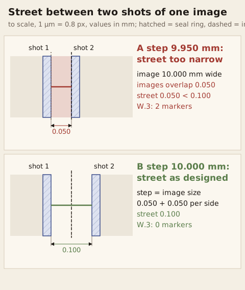
The figure shows a 0.300 mm window at the boundary between two shots. The hatched bars are the seal rings of the two facing dice, the dashed lines the image edges. LayoutEditor checked both cases on the simulated wafer: with a step of 9.950 mm rule W.3 of the wafer rule file below reports two markers, one per facing pair of dice; with a step of 10.000 mm it reports none.
Building and checking the reticle cell in LayoutEditor
The LayoutScript functions below build the three cells from an existing die cell. image() places the dice as one array reference and draws the image outline on layer 10/0, a construction layer that is not written. reticle() places images at their plate positions. wafer() steps one image across a square matrix; it is the simulation, not data for the shop.
from LayoutScript import *
MM = 1000000                      # 1 mm in database units of 1 nm; all values at 1x wafer scale

def image(d, die, name, nx, ny, pitch):
    # nx x ny dice on the die pitch; the outline on 10/0 is the image size for the stepper job
    img = d.addCell().thisCell; img.cellName = name
    x0, y0 = -(nx - 1) * pitch // 2, -(ny - 1) * pitch // 2
    img.addCellrefArray(die, point(x0, y0), point(x0 + pitch, y0 + pitch), nx, ny)  # 2nd point: 2nd column/row
    img.addBox(-nx * pitch // 2, -ny * pitch // 2, nx * pitch, ny * pitch, 10)
    return img

def reticle(d, placed):
    # every image at its place on the plate; this cell name goes on the mask order
    ret = d.addCell().thisCell; ret.cellName = "RETICLE_LAYOUT"
    for img, x, y in placed: ret.addCellref(img, point(x, y))
    return ret

def wafer(d, img, step, n, shift=0):
    # simulation of the stepper job: n x n shots of one image; never sent to the mask shop
    waf = d.addCell().thisCell; waf.cellName = "WAFER_LAYOUT"
    x0 = -(n - 1) * step // 2 + shift
    waf.addCellrefArray(img, point(x0, x0), point(x0 + step, x0 + step), n, n)
    return waf
The second point of addCellrefArray is passed as the position of the second column and second row, origin plus pitch. The test layout uses two images: IMAGE_A with the 2 × 2 dice, centered at x = −2.000 mm, and IMAGE_B, a test image 3.000 mm wide with 40 probe pads, centered at x = +5.500 mm. The rule file checks the reticle cell against the PAS 5500/300 field. The field outline comes from a second file, field_pas5500.gds, so that it never becomes part of the reticle data:
units 1e-6
grid 0.005 um
mode flat
source RETICLE_LAYOUT
gds tool = "field_pas5500.gds"
layer print = input(1).raw | input(2).raw | input(3).raw   # pads, seal ring, core
layer image = input(10).raw                               # image outlines, not written
layer field = input(11, 0, from=tool)
check "RET.1" "image outside the exposure field" : area(not_inside(image, field)) > 0 um2
check "RET.2" "chrome between images below 1 mm" : space(image) < 1000 um
check "RET.3" "printing data outside every image" : area(not_inside(print, image)) > 0 um2
input(n).raw reads the shapes without merging them first; none of the shapes in this layout overlap. not_inside(a, b) keeps the shapes of a that have a vertex outside every shape of b; the field is convex, so the vertex test is exact here. RET.3 finds printing shapes that no blade window opens, for example a label placed in the chrome between two images. Four variants of the test layout give these markers (RET.1, RET.2, RET.3):
reticle.ledrc on RETICLE_LAYOUT (markers RET.1 RET.2 RET.3):
  ok     0 0 0
  gap    0 1 0
  stray  0 0 1
  wide   1 0 0
gap moves IMAGE_B 0.500 mm closer to IMAGE_A. stray adds a 0.200 mm square on layer 1 in the chrome between the images. wide makes IMAGE_A 4 × 2 dice wide; its left edge at x = −14.000 mm lies outside the field edge at −11.000 mm. The same rule file with source WAFER_LAYOUT reports 120 RET.1 markers: of the 121 shots in the simulation only the center shot lies inside one exposure field. This is the result a shop would get if the wafer cell were named as the top cell of a stepper reticle.

The picture shows RETICLE_LAYOUT with the field outline loaded for display. The two navy rectangles are the image outlines; the empty area between and around them is chrome on a dark-field plate. The two images and the gap between them span 14.000 mm of the 22 mm field width.
Counting dice on a simulated wafer
The second rule file runs on WAFER_LAYOUT: a 100 mm wafer outline on 12/0, the usable area on 13/0, and IMAGE_A stepped 11 × 11 on a pitch equal to its image size, with the center shot on the wafer center. It counts complete dice and the shots that carry at least one of them, and checks the street between dice of neighboring shots:
units 1e-6
grid 0.005 um
mode flat
source WAFER_LAYOUT
layer seal = input(2).raw
layer image = input(10).raw
layer usable = input(13).raw
layer die = extents(seal)
layer full = inside(die, usable)
layer shots = interacting(image, full)
check "W.1" "complete die inside the usable area" severity info : area(full) > 0 um2
check "W.2" "shot with at least one complete die" severity info : area(shots) > 0 um2
check "W.3" "scribe between dice below 100 um" : space(die) < 100 um
extents(seal) turns each seal ring into the full die square. W.1 and W.2 have severity info: the report counts their markers as infos, and the exit code still counts every marker, so a run that finds complete dice exits with 1. Results for three grid positions and the two step cases of the previous section:
wafer.ledrc on WAFER_LAYOUT (W.1 dice, W.2 shots, W.3 scribe):
  ok       240 69 0
  shift55  240 68 0
  shift25  241 69 0
  step995  8 2 2
  step1000 8 2 0
estimate 235.8| Grid position (job "cell matrix") | Complete dice | Shots with a complete die |
|---|---|---|
| center shot on the wafer center | 240 | 69 |
| shifted 5.0 mm in x and y | 240 | 68 |
| shifted 2.5 mm in x and y | 241 | 69 |
A script without LayoutEditor, which tests the four corners of every die against the 47 mm radius, gives the same three pairs of numbers. The textbook estimate for gross dice per wafer, π·d²/(4S) − π·d/√(2S) (Hennessy and Patterson), gives 235.8 for d = 94 mm and a die pitch area S of 25 mm². The estimate ignores the grid position; the exact count depends on it, and the shift is a job parameter, not a property of the reticle. In this example the shift changes the count by one die and the number of shots by one.
Failure modes
| Failure | Cause | Check |
|---|---|---|
| Shop writes the whole wafer cell, or the wrong cell | top cell on the order is the wafer or die cell | order names RETICLE_LAYOUT; RET.1 with that source |
| Image cut off at the field edge | image plus gaps larger than the tool's field | RET.1 against the field of the named stepper |
| Light from a neighboring image | chrome between images below the tool's minimum | RET.2 |
| Test structure or label never exposed | printing shape outside every image outline | RET.3 |
| Streets of 50 µm or 150 µm between shots | job step differs from the image size | step = image size; W.3 on a simulated wafer |
| Features 4 times too small on the wafer | plate written 1:1 for a 4x tool | data at 1x; reduction stated on the order |
| Features 4 times too large on the wafer | data enlarged 4x in the file and again by the shop | data at 1x; no scaling in the file |
| Pattern shifted on the plate | shop centers the data automatically | origin at the plate center; "no automatic centering" on the order |
| Chrome missing between images | clear-field polarity chosen for a stepper plate | "polygons clear" or chrome drawn between images |
Checks before ordering
- The file contains one top cell for the reticle, named on the order, at 1x wafer scale, with the origin at the plate center.
- The rule file with that cell as
sourcereports 0 markers for RET.1, RET.2 and RET.3, using the field and chrome width of the stepper that will expose the wafers. - The order states the reduction, the stepper model for the template, polarity, reading direction, grade at reticle scale, and the barcode text.
- Every image size and image position in the reticle cell is copied into the job's image definition; the job's step equals the image size unless the street is designed for another step.
- A wafer simulation with the planned step, matrix shift, and edge clearance reports the expected number of complete dice and no W.3 markers.
Continue exploring
-
 Steppers and why size matters
The machine prints a field, then steps. Your die has to fit that window, not only the wafer.
-
 Cell arrays and step-and-repeat: rows, columns, pitch, and AREF
An array places one cell in rows and columns at a fixed pitch and is stored as one array reference (AREF in GDSII). How a wrong step adds up across the grid, and why one record has one rotation.
-
 What is a photomask? The glass plate that prints a chip
A photomask, also called a reticle, is a quartz plate with a chrome pattern. Light shines through it to copy one layer of a chip onto a wafer, and a chip needs a stack of them.
-
 Naming the top cell you ship
A top cell is a cell that no other cell places; a mask shop or shuttle builds from exactly one, under the name it asks for, and a GDSII file has no record that marks it.
-
 Alignment marks and registration
Alignment marks are paired shapes on two mask levels that let an aligner, stepper, or writer place each new level on the pattern already on the wafer.
-
 Cells and instances
Draw the pad once and stamp it many times. Each stamp is the same drawing in a new place, not a photocopy of the ink.
-
 Mask fracture in one sitting
Your polygons become the shots a mask writer can fire. The file grows. Slivers appear.
-
 From idea to something a shop can print
How a napkin sketch becomes a file, a cover letter, and a glass plate a shop can print from.