
glossary
Stackup
Stackup is the agreed sandwich of a board or a tiny circuit: which sheets exist, how thick they are, and in what order.
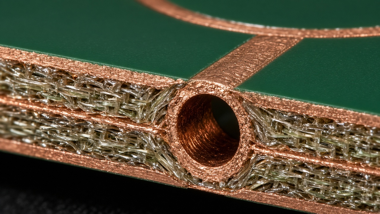
The edge of one board: woven fiberglass, copper sheets, and a plated hole.
Impedance, cost, and warpage live in that sandwich, not in a pretty 2-D view. A four-layer board might be signal, ground, power, and signal, with 0.2 millimeter cores and 1 oz copper. A chip stackup is a count of metal layers, plus oxides and passivation. If you route a 50 ohm line on a stackup the shop cannot build, the line is not 50 ohms. The table reads L1 35 µm Cu, 0.1 mm prepreg, L2 35 µm Cu…, or the foundry shows a cross-section with eight metals.
On a PCB, the stackup names soldermask and silkscreen too. Export Gerber files in that order and label them. On a chip, the stackup lives in the PDK. You do not invent metal 9. Drawing inner-layer copper as if it were free, then learning the shop’s cheap stackup has no inner layers, is the usual miss. Ask before you pour.
Impedance calculators need the stackup, not a guess. A 0.15 millimeter-wide line over a 0.1 millimeter dielectric is not the same as the same line over 0.2 millimeter. A shop can change foil weight and quietly move a 50 ohm pair. Freeze the stackup in the purchase order. Chip people freeze metal counts the same way in the PDK.
The sandwich, the cross-section, and the copper are covered in a PCB stackup, looking at a cross section, and PCB copper is also a layer.