
glossary
PCB
A PCB (printed circuit board) is a board that holds parts and conducting roads, built from stacked sheets of conductor and insulator instead of a silicon sandwich.
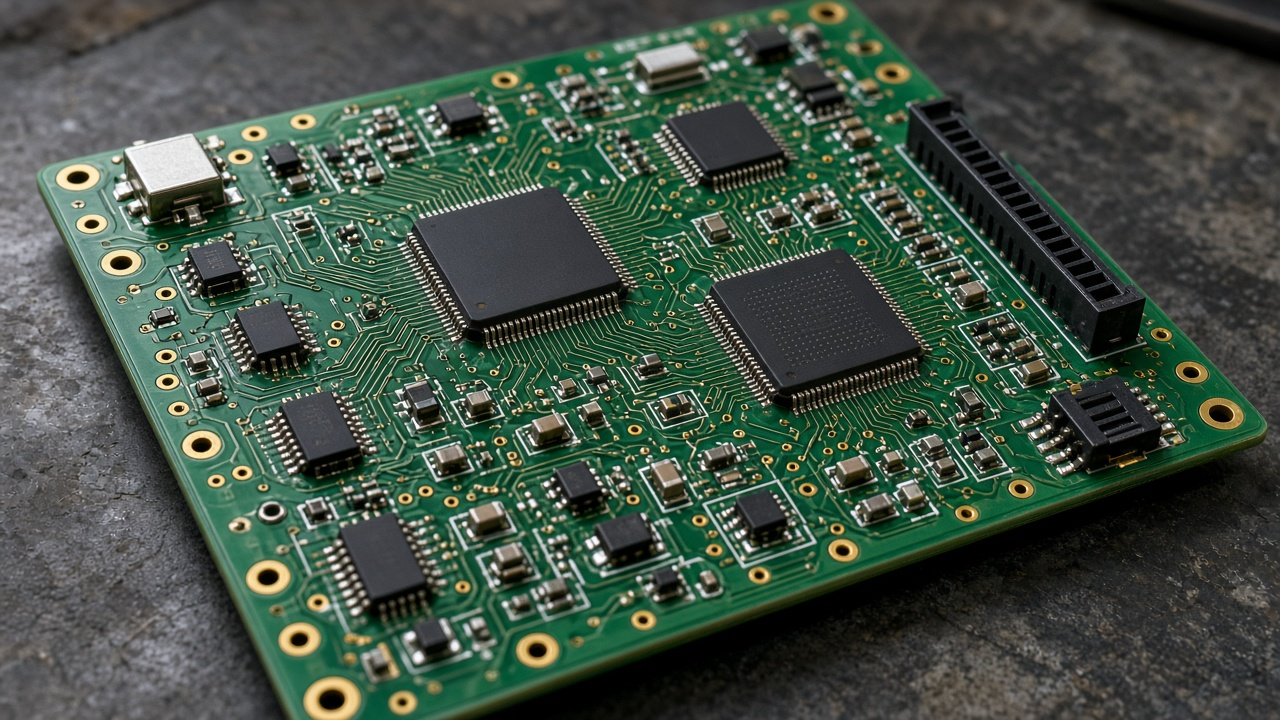
A board that holds parts, built from stacked sheets rather than a silicon disk.
The craft is the same idea as a chip drawing, carried out for different shops. The drawing still uses layer stacks, still obeys width and spacing, and still exports files a factory will build. The factory wants Gerber plots, drills, and a stackup, not a GDSII phone chip. A 0.2 millimeter trace on 1 ounce copper is a normal conversation. The object in hand is a green, black, or white rectangle with silver pads and tiny letters. In the editor the same board is copper, soldermask, silkscreen, and holes.
A part landing is a footprint. A schematic still says what is connected. Board tools often flatten copper art. Chip tools hoard hierarchy. Treating the file as a photograph of the finished board misses the split. The soldermask color is a shop option. The copper shapes are the instruction.
A board library of footprints is as important as the copper art. A 4-layer job is quoted cheaper than a 6-layer job, and a 0.1 millimeter via is a hole one shop will drill and another will refuse. The schematic still comes first. A correct board with a wrong net is a working heater. Export plots, drills, and a stackup note together. What those copper sheets are is a PCB stackup. What the shop needs in the parcel is sending a board to a PCB fab. The same idea of sheets and shapes, before the board diverges, is what is a layout.