
glossary
Soldermask
Soldermask (solder resist) is the coating that covers conducting foil you must not solder, with openings where solder is allowed to sit.
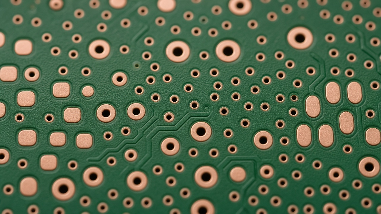
Green coating over the foil, with openings where solder is allowed to sit.
A board without a correct mask is a short waiting for a blob of solder. The mask is its own layer in the stackup. Openings are often a little larger than the pad so the copper lands stay wettable. A 0.05 millimeter expansion is a typical shop number. Tiny openings over traces are how solder is kept from climbing a via. On the finished board the film is green, or some other color, with windows on the pads. In the editor the mask may appear as a negative: openings are drawn, or the mask is drawn and the pads are subtracted, depending on the tool.
Mask is not silkscreen. Silk is ink for humans. Mask is a process film. Copper under intact mask should not take solder. Mask expansion and the web, the sliver of mask between pads, have minima. Two 0.25 millimeter pads on a 0.4 millimeter pitch can lose the web, so solder bridges. Tented vias hide copper from the iron. Open vias are test points. Put that choice in the footprint, not in a last-minute edit on the board layer only.
Sending copper Gerbers and forgetting the mask files leaves the shop to guess, or to stop. Tenting a via that a test probe needed open is the other miss.
The sandwich, the fab pack, and the copper are covered in a PCB stackup, sending a board to a PCB fab, and PCB copper is also a layer.