
glossary
Copper
Copper is the reddish conductor on a printed circuit board: the foils and plated holes that carry current, drawn as shapes on those foil sheets.
A board is a copper drawing first. Traces, planes, pad lands, and poured fills are copper. Thickness is spoken in ounces: 1 oz is about 35 micrometers. A 0.2 millimeter trace on 1 oz copper has a current story and a shop story. Inner copper and outer copper are different layer names in the stackup. In the editor the shapes are salmon or orange; on a stripped board they are dull metal. A ground plane is a big copper polygon with hole cutouts for vias and keep-aways. Chip metal is the cousin. Gerber plot files carry the copper art after the tool flattens it. Soldermask covers copper you must not solder. The green color of a finished board is usually that mask. Copper lives underneath, and on the pads where the mask opens.
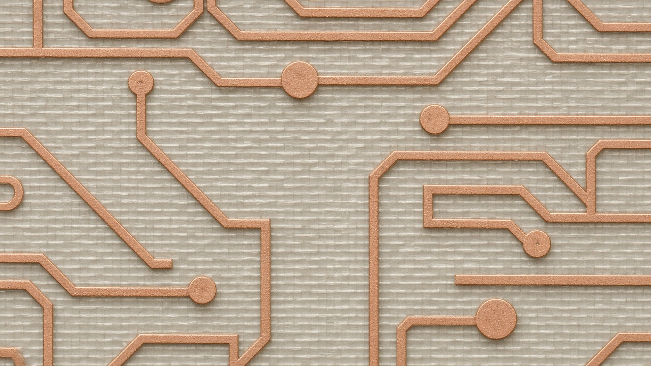
Bare foil traces and round pads, before any green coating.
How the foil is drawn as a layer, how a board stack names it, and what a layer is for are covered in PCB copper is also a layer, a PCB stackup, and what a layer is for.