
glossary
Gerber
Gerber is a plot language that tells a board camera or a printer how to flash foil, ink, and protective coating, one sheet at a time.
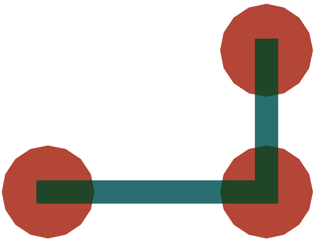
Round flashes are the pads. The ribbon between them is a draw.
A printed circuit board house rarely wants a chip stream. It wants a set of plot files plus drills. Each file is one layer of the stackup: top copper, inner copper, soldermask, or silkscreen. Modern Gerber, called X2, can label those jobs. Older Gerber is a series of flashes and draws with no names attached. On disk the set looks like board.gtl, board.gbl, and the companion files, or like one .gbr per sheet. A 0.3 millimeter trace is a draw made with a 0.3 millimeter aperture. A round pad is a flash of a 0.8 millimeter circle.
Gerber is not a cell tree. The hierarchy is usually already gone, which is why board tools often flatten before export. Mechanical outlines sometimes travel as DXF beside the plots. One plot file is not the board. The shop needs every sheet, the drill file, and a note that says which file is which. A missing soldermask file is a board full of bare copper.
X2 attributes can name a file TopCopper or BotSolderMask. Use them. A shop ticket may still map job.gts to the top mask because someone followed an old suffix table. Ship a README that states the units in millimeters, includes a stackup sketch, and says whether the holes are plated. Zip the plots and the drills together so one sheet cannot wander off alone.
See Gerber is a plot language, a PCB stackup, and sending a board to a PCB fab.