
glossary
Silkscreen
Silkscreen (silk) is ink printed on the board for humans: part outlines, reference names, logos, and polarity marks.
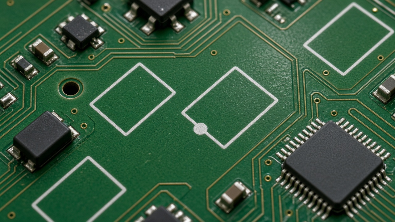
White ink outlines and a polarity dot. The marks are for a person, not a conducting path.
Silk does not conduct and does not solder, yet it causes assembly mistakes when it lies. A pin-1 dot on the wrong end is a whole reel of parts rotated. Silk that floods a pad can block solder. Shops often clip silk from pads automatically. Do not rely on that kindness. On the board the ink shows as white letters R12 and U3, a diode band, and a footprint box. A 1 millimeter-tall reference is readable. Text at 0.4 millimeter is hope. Keep text 0.8 millimeter or taller when you can.
Silk is a layer in the stackup, plotted as Gerber the way copper and soldermask are plotted. It is the board cousin of text on a layout. Chip documentation layers are the same idea: for people, not for chrome. A courtyard and courtyard clearance are CAD rules. Silk is paint. If the ink is skipped to save a screen, the courtyard should still be true. Legal marks that live only in silk disappear with that screen.
Assembly also reads silk for polarity and pin 1: a stripe on a diode footprint and a notch on an IC. If the shop skips silk to save a screen, those marks must still exist as copper features or as a pick-and-place file. Gerber silk files are easy to omit from a zip. Check the pack list.
The sandwich, the fab pack, and the lettering are covered in a PCB stackup, sending a board to a PCB fab, and text on a layout.