
Shapes · Chips
Vias and contacts in IC layout: cut layers, enclosure, and via rows
Vias and contacts in a chip layout: the cut layers between floors, SKY130 via size, spacing and enclosure rules, via rows, and what a DRC cannot see.
Last edited: October 12, 2026

A chip is wired on several floors. Polysilicon gates and doped silicon sit at the bottom, and stacked metal layers run above them, each separated from the next by a sheet of insulating glass. A wire on one floor cannot reach a wire on another floor by crossing it, because the glass between them is in the way. A cross-section through the film stack shows those floors and the glass between them in height, which the top view of a layout does not store. The connection is a small square hole etched through that glass and filled with metal. When the hole joins two metal layers it is called a via. When it joins the first wiring level down to a gate or to the silicon itself it is called a contact. In a layout file both are drawn the same way: a small square on a layer of its own, a cut layer, placed where the shapes above and below overlap.
The picture at the top is one signal climbing from a transistor gate to the second metal layer of the open SkyWater SKY130 process, drawn in LayoutEditor and checked with the rule decks on this page without a single marker. Read it left to right. The plum finger at the bottom left is polysilicon; its square pad holds the black licon, a 0.170 µm contact up to the teal local interconnect (li1). The teal strap carries the signal to the amber mcon, another 0.170 µm cut, up to the blue metal 1 (met1). The blue strap carries it to the purple via, a 0.150 µm cut, up to the orange metal 2 (met2), which leaves the picture at the top. Three cuts, three floors, and every cut sits inside the shape below it and the shape above it.
The stack of cuts in one real process
Every process names its cut layers and gives each one fixed numbers. SKY130 is a useful example because its rule tables are public. The table below lists its cuts from the bottom up, with the GDSII layer/datatype pair where the cut is drawn (datatype 44 marks a cut, 20 a drawn wiring shape; see GDS layer and datatype).
| Cut | Joins | GDS layer | Size (min = max) | Cut-to-cut space |
|---|---|---|---|---|
| licon | diffusion, tap or poly to li1 | 66/44 | 0.170 µm (licon.1) | 0.170 µm (licon.2) |
| mcon | li1 to met1 | 67/44 | 0.170 µm (ct.1) | 0.190 µm (ct.2) |
| via | met1 to met2 | 68/44 | 0.150 µm (via.1a) | 0.170 µm (via.2) |
| via2 | met2 to met3 | 69/44 | 0.200 µm (via2.1a) | 0.200 µm (via2.2) |
| via3 | met3 to met4 | 70/44 | 0.200 µm (via3.1) | 0.200 µm (via3.2) |
| via4 | met4 to met5 | 71/44 | 0.800 µm (via4.1) | 0.800 µm (via4.2) |
By that naming, licon and mcon are the contacts and via through via4 are the vias. Other processes draw the line in other places, and many older ones have no local interconnect at all, so "contact" there means the single cut from metal 1 down to silicon or poly. The idea does not change: one cut layer per pair of neighboring floors, and a cut only connects the two floors it is named for. A path from poly to met2 needs every cut in between, which is exactly what the lead picture shows.
Why a cut is a fixed square
The size column says "min = max" for a reason. The SKY130 table gives the width of a via as both a minimum and a maximum, and rule via.3 adds that only minimum-size square vias are allowed outside the die seal ring (ct.3 says the same for mcon). A hole of one size etches through the glass at one rate and fills completely, so every cut on the die comes out the same. A larger hole would etch differently and might not fill to the top. The consequence for the person drawing is simple: you never make a connection stronger by drawing a bigger cut. You draw more cuts of the same size.
The landing: enclosure on both floors
A cut has to land on metal at the bottom and be covered by metal at the top, with some margin, because each mask layer is aligned to the others only to within a small error. That margin is the enclosure. For the SKY130 via it is set twice, once for each floor: met1 must enclose a 0.150 µm via by at least 0.055 µm on every side (via.4a), and by at least 0.085 µm on one of every two adjacent sides (via.5a). Met2 has the same pair of numbers for the same via (m2.4 and m2.5). The mcon one floor lower uses 0.030 µm and 0.060 µm (m1.4, m1.5), and li1 only has to reach the edge of an mcon (ct.4, 0.000 µm).
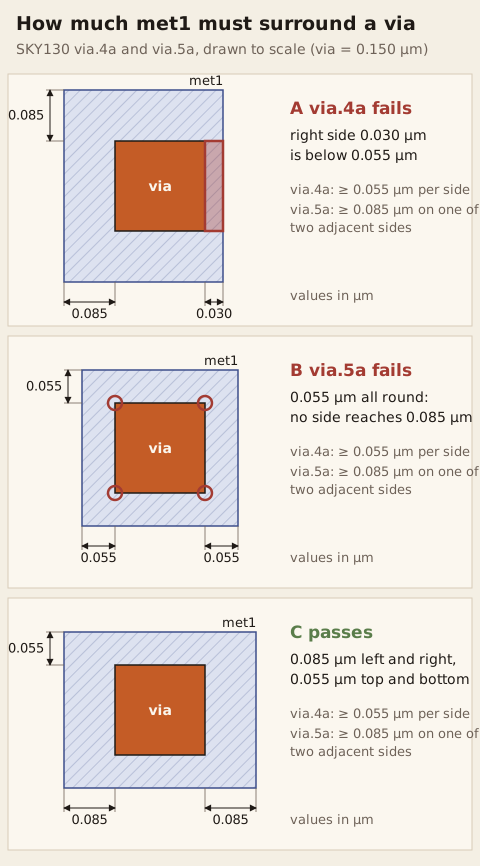
The diagram shows the met1 side of that rule, drawn to scale at 1 µm = 600 px. In A, the right side has only 0.030 µm of metal beyond the via, below the 0.055 µm minimum, and the red band marks that side. In B, the metal is an even 0.055 µm all round: every side meets via.4a, but no side reaches 0.085 µm, so each of the four corners has two thin sides meeting, and each corner is circled. C passes both rules with 0.085 µm on the left and right and 0.055 µm on top and bottom, which is the shape a via takes in a minimum-width wire. The same geometry was written to a GDS file and checked with a hand-written rule deck; LayoutEditor reported one via.4a marker for A, four via.5a markers for B and none for C, exactly what the figure claims. How the "adjacent sides" rule is written as one check line is the subject of One of two adjacent sides.
Rows and arrays: more cuts, not bigger ones
Because the cut size is fixed, a wide wire carrying real current is tied to the next floor with a row or a grid of cuts. Each cut adds a parallel path, so the resistance of the joint falls roughly with the number of cuts, and the current through each one falls with it. A row also keeps the connection alive if one cut prints small or fails to fill, which is why many flows add a second cut even where one would carry the signal. For SKY130 vias the row pitch is the cut plus the space, 0.150 + 0.170 = 0.320 µm.
A row is easy to draw by hand and easier to draw with a script. This is LayoutScript, the Python interface of LayoutEditor, drawing a met1 strap, a met2 strap on top of it and eight vias between them:
from LayoutScript import project

M1, VIA, M2 = 68, 68, 69          # GDS layers; datatype 20 = drawing, 44 = cut
CUT, SPACE, ENC = 150, 170, 85    # nm: via size, via-to-via space, enclosure
N = 8                             # vias in the row

layout = project.newLayout()      # database unit 1 nm
cell = layout.drawing.currentCell
cell.cellName = "via_row"

length = ENC + N * CUT + (N - 1) * SPACE + ENC
height = ENC + CUT + ENC
cell.addBox(0, 0, length, height, M1).setDatatype(20)
cell.addBox(0, 0, length, height, M2).setDatatype(20)
for k in range(N):
    x = ENC + k * (CUT + SPACE)
    cell.addBox(x, ENC, CUT, CUT, VIA).setDatatype(44)

layout.drawing.saveFile("via_row.gds")
All lengths are integers in the database unit of 1 nm, so the 0.085 µm enclosure is written as 85. The strap comes out 2.560 µm long and 0.320 µm tall. Run through the deck in the next section, it produces no marker. In a large design the same row is usually kept as its own cell and placed as an instance wherever two straps meet, so a change to the cut pattern reaches every copy at once.
What a rule check sees, and what it cannot
A design rule check (DRC) measures shapes against the factory's rules (see DRC is a spellchecker). For the via, the rules fit in one short LayoutEditor deck in the .ledrc format:
units 1e-6

layer m1  = input(68, 20)
layer via = input(68, 44)
layer m2  = input(69, 20)

# the cut itself: exactly 0.150 um square, 0.170 um apart
check "via.1a" "via.1a : via width >= 0.150 um"  : width(via) < 0.15 um
check "via.2"  "via.2 : via spacing >= 0.170 um" : space(via) < 0.17 um

# the landing below: met1 around the via
check "via.4a" "via.4a : met1 enclosure of via >= 0.055 um" : enc(m1, via) < 0.055 um
check "via.5a" "via.5a : met1 enclosure of via >= 0.085 um on one of two adjacent sides" : enc(m1, via) < 0.085 um rect_sides=1,2
layer via_off_m1 = via - m1
output via_off_m1 "via.4a" "via.4a : via not covered by met1"

# the landing above: met2 around the same via
check "m2.4" "m2.4 : met2 enclosure of via >= 0.055 um" : enc(m2, via) < 0.055 um
check "m2.5" "m2.5 : met2 enclosure of via >= 0.085 um on one of two adjacent sides" : enc(m2, via) < 0.085 um rect_sides=1,2
layer via_off_m2 = via - m2
output via_off_m2 "m2.4" "m2.4 : via not covered by met2"
Each layer line names a GDS layer/datatype pair, and each check line is one row of the rule table with its ID, a message and a condition. The two layer … = via - m1 lines matter more than they look. The enclosure measurement enc() only judges a cut that lies inside the outer shape, so a via that hangs off the edge of a strap, or sits in the gap between two straps, would pass the enclosure lines unseen. Subtracting the metal from the via leaves exactly the uncovered part, and output turns it into a marker under the same rule ID. The deck runs from the command line:
layout --drc via_met1_met2.ledrc via_row.gds --outdir=drc_outchecks 6
errors 0
The second picture shows the deck at work on four cases, with every red shape a marker LayoutEditor wrote. Top left is the legal crossing: one purple via inside a blue met1 strap and an orange met2 strap, no marker. Bottom right is a row of four vias only 0.160 µm apart; each of the three gaps is below the 0.170 µm of via.2 and gets a marker. Bottom left is a via drawn in the empty space between two parallel straps; it touches neither, and the coverage lines flag it once for met1 (via.4a) and once for met2 (m2.4).
Top right is the case that matters most, and it has no marker at all. The square at the crossing was drawn on the met1 layer instead of the via layer. On screen it looks like a joint; in the file it is just a little more met1, merged into the strap below. There is no cut, so there is nothing for a via rule to measure, and every rule is satisfied. The two straps cross without ever touching, and the net is open.
The check that finds a missing cut
A missing cut is not a geometry error, it is a connectivity error, so it is found by the check that compares connectivity: layout versus schematic (LVS, see LVS: layout versus schematic). LVS follows the shapes from floor to floor through the cut layers to build a netlist and compares it with the circuit; a net that the schematic joins and the layout does not shows up as an open or a missing connection. Two habits catch the same mistake earlier. Hide every layer except the cut layers before calling a block done: each joint you meant to make should still show a square, and a square that vanishes with the metal was never a cut. Then switch the metals back on and confirm that every cut lands on both floors it is named for.
Vias and antenna rules
Cuts also matter while the chip is being built. Metal is etched in a plasma, and a long wire connected to a transistor gate collects charge during that etch; if it collects too much, the charge can damage the thin gate oxide. Foundries limit the ratio of exposed conductor area to the gate area it is connected to, the antenna ratio (see Antenna rules: charge during etch). The SKY130 limits without a protection diode are 400 for met1 and met2 and 6 for the via, 3 for mcon and licon. As a rough guide from the same tables, a minimum-width met1 wire on a 1 µm² gate may run about 570 µm before it violates, and about 4,280 µm with a 1 µm² diode.
Vias give the standard fix. A layer only counts while it is being etched, and at that moment only what is already connected through the floors below is attached to the gate. If a long met1 run is cut short of the gate and the last stretch is bridged on met2, the long met1 piece is not attached to the gate while met1 is etched. By the time met2 is etched and joins the two pieces, the met1 is buried under glass and collects nothing; only the short met2 bridge is exposed. The detour costs two vias and a short piece of upper metal, and it is often cheaper than a diode.
The same idea outside chips
A printed circuit board uses the same word for a drilled and plated hole. A through-hole via joins all copper layers, a blind via starts at an outer layer and stops inside, a buried via joins only inner layers, and a laser-drilled microvia joins neighboring layers in fine-pitch boards. The size of a board via is set by the drill, not by a cut-layer rule table, and it is far larger than anything in the table above, but the drawing logic is the same: a hole that connects only the layers it passes through, with a copper ring around it on each layer that plays the role of enclosure (see A PCB stackup).
A short checklist
Before you call a connection done, check four things. The square is on the cut layer named for the two floors you are joining, not on one of the metals. Every cut is the one allowed size, with at least the minimum space to its neighbors (0.170 µm for the SKY130 via). Each cut is covered on both floors with the required enclosure (0.055 µm everywhere and 0.085 µm on one of two adjacent sides for the via, in met1 and met2 alike). And a joint that carries current has a row of cuts, not one. The first of these is the one no geometry rule will catch for you.
Continue exploring
-
 Enclosure is a frame for misalignment
The inner feature has to sit on an island big enough that the factory’s slop cannot knock it off.
-
 What a layer is for: layer numbers, purposes, and hiding sheets
A layer is a sheet the factory spends a process step on. GDS layer/datatype pairs with real SKY130 numbers, drawn vs derived layers, and why hiding a layer is a filter, not a delete.
-
 Width and space
The two oldest rules: don’t be skinny, don’t cuddle. Everything else is a variation.
-
 Cells and instances
Draw the pad once and stamp it many times. Each stamp is the same drawing in a new place, not a photocopy of the ink.
-
 Overlapping is not merging
Two shapes sharing coordinates are still two objects. A merge is one outline. Factories care which you meant.
-
 Looking at a cross-section
A side view of the sandwich. Layout is the top of this. MEMS people live here.
-
 One of two adjacent sides: checking m1.5, li.5, and via.5a in .ledrc
Some contact rules let the metal be thin on one side, or on two opposite sides, but never on two sides that meet at a corner. How to read that rule in the SKY130 table, write it by hand as one LayoutEditor check line, and prove it on a layout built to fail.
-
 Antenna rules: charge during etch
Antenna rules limit the conductor area connected to a transistor gate during manufacturing, because plasma etching charges the wire; jumpers and antenna diodes fix violations.