
Masks · Layers · Combining shapes
Derived layers: when a mask is a boolean
Some masks are computed from drawn layers with boolean operations and sizing; the SKY130 N+ implant recipe shows the steps, and a LayoutEditor rule file reproduces and checks them.
Last edited: November 10, 2026

A generated mask layer (also called a derived mask layer) is mask data that a program computes from drawn layers with boolean operations, sizing, and selection. A foundry builds some of its masks directly from one drawn layer, some from a drawn layer plus computed additions, and some only by computation, with no drawn layer behind them. Mask data preparation, also called layout post-processing, is the step that turns the polygons of the submitted GDSII or OASIS file into mask-writer data; generated layers, seal rings, fill, optical proximity correction, and fracturing all belong to it (Lienig and Scheible, Fundamentals of Layout Design for Electronic Circuits, 2020, ch. 3.3). This article covers masks built from other layers. The derived layers that DRC and LVS decks compute for checking, such as gate = poly & diff, are described in boolean operations.
The picture at the top is a LayoutEditor view of eleven SkyWater SKY130 high-density standard cells placed in three abutted rows; the middle row is mirrored, as in a placed block. Green is drawn diffusion, red is drawn polysilicon, and the dotted background is drawn n-well. The blue grid is an N+ implant mask and the orange grid a P+ implant mask. Nobody drew these two layers: the five-step rule file of this article computed them from the diffusion and the n-well. Their outlines follow the diffusion at a fixed distance. The white strip just below the center, enclosed by P+ on all sides, is a hole of 1.336 µm²; it is larger than the minimum hole area, so the recipe keeps it open. The other white areas lie between the two masks and receive neither implant.
Drawn, generated, or both
The GF180MCU design manual lists 33 mask layers by reticle number (section 4.3, "Mask Layer Numbering"). Each row states whether the mask is drawn, generated, or both, its digitized polarity, and the GDS layer number of the output:
| Source of the mask | Masks | Examples (mask number, polarity) |
|---|---|---|
| Drawn | 15 | Poly2 (60, Chrome), Contact (75, Clear), Via1 (85, Clear), Nplus (65, Clear) |
| Drawn + Generated | 12 | COMP (10, Chrome), Nwell (5, Clear), LVPWELL (18, Chrome), Pplus (70, Clear), Metal1 (80, Chrome) |
| Generated | 6 | AD planarization aid (11), TP 3.3 V PMOS Vt implant (64), TN 3.3 V NMOS Vt implant (61), MVNVT (1L), MVPVT (2E), PIB bond and passivation opening (99), all Clear |
Polarity states whether the digitized area becomes chrome or clear on the plate; a contact or via mask is written as clear openings, a metal mask as chrome lines. The manual defines the generated layers in section 4.2 only by reference: "Please refer to the generation algorithm spec: YI-141-GR065 or GR-000179." That specification is not part of the published manual. A designer therefore cannot reproduce a generated mask such as TN, the 3.3 V NMOS threshold-voltage implant, from the manual alone.
What the manual does publish is a Topological Truth Table (section 4.4). For each device type it lists, per drawn and marking layer, 0 (the layer must not touch the structure), 1 (the layer must enclose or match it), X (no electrical effect), or Op (optional). The row for a 3.3 V NMOS outside deep n-well reads COMP 1, POLY2 1, Nplus 1, Nwell 0, DNWELL 0, Dualgate 0, LVPWELL X. The note under the table states that LVPWELL is a generated layer in this process: NMOS devices are drawn in the p-substrate and the p-well is computed. The table states the result that the generation must reach. The manual adds that anyone who uses other algorithms to generate implant layers should use the table to confirm that each structure receives the specified implants.
What SKY130 creates
The SkyWater SKY130 Layers Reference contains a Mask Generation table (Table F2b) with one column per mask and one row per device. Its legend reads: "D = DRAWN indicates that a layer is drawn by Design. C = CREATED indicates that the layer is only created by CAD." In the row for the 1.8 V NMOS sky130_fd_pr__nfet_01v8, three masks carry a C: FOM (field oxide), P1M (poly), and NSDM (N+ implant). The row for the 1.8 V PMOS sky130_fd_pr__pfet_01v8 carries a C in seven columns: FOM, NWM, HVTPM, NCM, P1M, NTM, and PSDM. HVTPM is the high-Vt PMOS implant mask; the table lists it as created for the standard 1.8 V PMOS as well.
The GDS layer table of the same reference separates the drawing layers from mask-level data. Mask-level layers carry a c prefix and datatype 0, and some have purposes for manual corrections:
| Mask | Mask-level layer | mask add | mask drop |
|---|---|---|---|
| field oxide (cfom) | 23:0 | 22:21 | 22:22 |
| N+ implant (cnsdm) | 30:0 | 29:21 | 29:22 |
| P+ implant (cpsdm) | 32:0 | 31:21 | 31:22 |
| poly (cp1m) | 28:0 | 33:43 | 33:42 |
| metal 1 (cmm1) | 36:0 | — | — |
A shape on a mask add layer adds area to the generated mask, and a shape on a mask drop layer removes area from it. These purposes let a designer correct a generated mask locally without changing the generation program. Reading a layer map explains the numbering of drawing layers and purposes.
A published recipe: the SKY130 N+ implant in Magic
The open-source layout editor Magic stores abstract layers, and its technology file computes the mask layers when it writes GDS. The Magic technology file manual states the reason: "The layers stored by Magic do not always correspond to physical mask layers. For example, there is no physical layer corresponding to … ntransistor; instead, the actual circuit must be built up by overlapping poly and diffusion over pwell." The open_pdks technology file for SKY130 (version 1.0.588-62-g1689ac3) generates the N+ implant layer NSDM (GDS 93/44) in its gdsii output style. All values in that style are in nanometers. Each operation corresponds to a SKY130 rule:
Operation in sky130A.tech |
Effect | SKY130 rule |
|---|---|---|
bloat-or allnactivenontap * 125 allpactivetap 0 |
grow n-diffusion by 125 nm, by 0 nm toward an abutting p-tap | n/psd.5a enclosure of diff 0.125 µm; n/psd.6 butting edge 0.000 µm |
bloat-or allnactivetap * 125 allpactivenontap 0 |
the same for n-taps | n/psd.5b enclosure of tap 0.125 µm |
bridge 380 380, then and-not basePSDM |
add material in corner gaps; remove it from the P+ area | n/psd.1 width 0.380 µm; n/psd.2 space 0.380 µm |
grow 185, shrink 185 |
merge shapes closer than 370 nm | n/psd.3 "Manual merge if less than minimum" |
close 265000 |
fill enclosed holes below 265,000 nm² | n/psd.11 hole area 0.265 µm² |
The manual describes two limits of the grow-and-shrink pair. close exists because "in some cases the minimum hole size is larger than the material spacing rule, and the grow/shrink pair of operators can then merge across areas where the material is prohibited." bridge exists because grow-and-shrink "will fail for geometry in a catecorner arrangement, either not closing the gap at all, or else generating a small sliver; a DRC width error or a DRC spacing error results." The bridge operator was added in Magic 8.3.24.
The recipe as a LayoutEditor rule file
The rule file below computes the N+ implant mask in five steps from SKY130 drawn diffusion (65/20) outside n-well (64/20) and writes it to the mask-level layer 30/0. It covers n-diffusion only: no taps, no butting edges, and no P+ mask. Steps 2 to 4 replace the Magic operations grow/shrink, bridge, and close with .ledrc operators. The checks at the end test the generated layer against the implant rules.
units 1e-6
layer diff  = input(65, 20)
layer nwell = input(64, 20)
layer nadd  = input(29, 21)
layer ndrop = input(29, 22)
layer ndiff = diff - nwell
# 1: n/psd.5a, implant encloses diffusion by 0.125 um
layer grown = merged(sized(ndiff, 0.125 um))
# 2: grow, merge, shrink closes gaps below 2 x 0.185 = 0.370 um
layer closed = sized(merged(sized(grown, 0.185 um)), -0.185 um)
# 3: bridge corner gaps below n/psd.2 0.380 um
layer gap = polygons(space(closed) < 0.38 um)
layer bridged = closed | sized(extents(gap), 0.19 um)
# 4: fill holes below n/psd.11 0.265 um2
layer filled = bridged | with_area(holes(bridged), 0, 0.265 um2)
# 5: designer adjustments
layer nsdm = (filled | nadd) - ndrop
output nsdm 30, 0
check "n/psd.1" "nsdm width 0.380 um" : width(nsdm) < 0.38 um
check "n/psd.2" "nsdm space 0.380 um" : space(nsdm) < 0.38 um
check "n/psd.10a" "nsdm area 0.265 um2" : area(nsdm) < 0.265 um2
check "n/psd.11" "nsdm hole 0.265 um2" : area(holes(nsdm)) < 0.265 um2
check "n/psd.9" "diff outside nsdm" : area(ndiff - nsdm) > 0 um2
target "nsdm_mask.gds"
with_area(holes(bridged), 0, 0.265 um2) keeps holes with an area of at least 0 and less than the limit; the upper bound is exclusive. The test layout has eight cases. "Grow only" is the same file with step 1 alone:
| Case | Drawn n-diffusion (µm) | Grow only | Five steps |
|---|---|---|---|
| single | 1.000 × 0.420 | 1 shape, 0.838 µm² | same |
| gap_0.55 | two 0.420 × 1.000, 0.550 apart | 2 shapes 0.300 apart, n/psd.2 1 marker | 1 shape, 2.050 µm² |
| gap_0.70 | two 0.420 × 1.000, 0.700 apart | 2 shapes 0.450 apart | same |
| corner_0.30 | two 0.420 squares, 0.300 apart in x and y | corners 0.071 apart, n/psd.2 2 markers | 1 shape, 16 vertices, 1.324 µm² |
| small | 0.150 × 0.150 | 0.160 µm², n/psd.10a 1 marker | same |
| small_add | as small, plus a 0.600 square on mask add 29/21 | 0.160 µm², n/psd.10a 1 marker | 0.360 µm² |
| drop | 1.000 × 0.420, plus a 0.500 wide strip on mask drop 29/22 over its right end | 0.838 µm² | 0.553 µm², n/psd.9 1 marker |
| ring_hole | frame of 0.300 wide bars around a 0.650 × 0.850 opening | hole 0.400 × 0.600 = 0.240 µm², n/psd.11 1 marker | hole filled, 2.550 µm² |
The five-step run reports two markers, both intended: the generation does not enlarge an island below the minimum area, and a mask drop over diffusion leaves diffusion without implant. The mask add square repairs the small island. The grow-only run reports six markers:
five steps:  checks 5, errors 2
small        n/psd.10a  1
drop         n/psd.9    1
grow only:   checks 5, errors 6
gap_0.55     n/psd.2    1
corner_0.30  n/psd.2    2
small        n/psd.10a  1
small_add    n/psd.10a  1
ring_hole    n/psd.11   1
Corner gaps
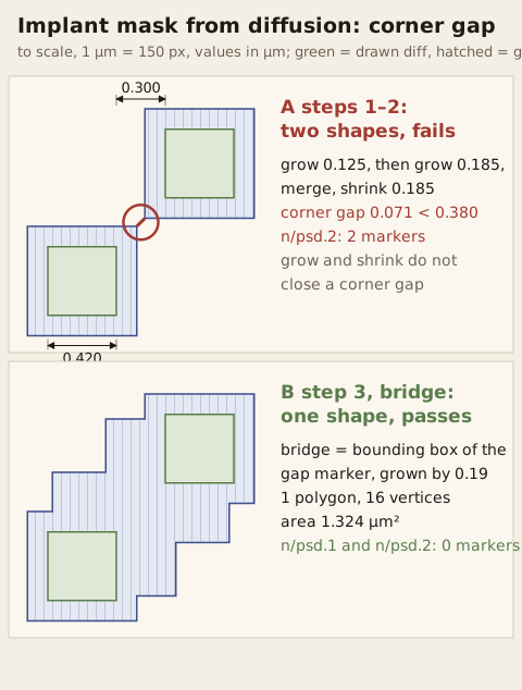
Panel A shows the corner case after steps 1 and 2. Grown by 0.125 µm, the two implant squares are 0.050 µm apart in x and in y, and their corners are 0.071 µm apart. The grow by 0.185 µm makes the squares overlap in a 0.320 µm square at the corner; the shrink removes that overlap again, because a square of that size is narrower than twice the shrink distance. The two shapes and the space violation remain, which is the catecorner case of the Magic manual. Panel B shows step 3. space(closed) < 0.38 um reports the gap as edge pairs, polygons turns them into area, extents takes the bounding box, and sizing by 0.19 µm, half the minimum width, makes the bridge at least as wide as n/psd.1 requires. The result is one polygon of 1.324 µm² with no marker. A bridge made of the raw gap polygons, without extents and sizing, joins the two shapes with a slanted strip: that variant reports eight n/psd.1 width markers at the corner, the narrowest at 0.055 µm.
On a placed block
The same five steps, written once for the N+ and once for the P+ implant (pdiff = diff & nwell, n/psd.10b area 0.255 µm²), ran on the block of the lead picture: eleven cells, 12.880 µm wide, 8.160 µm high. Nine checks (width, space, and area of both masks, overlap of N+ and P+, and diffusion outside its implant) reported no marker. The generated N+ mask has 2 polygons and 34.037 µm², the P+ mask 2 polygons and 42.194 µm².
The SKY130 library also draws implant layers in every cell, nsdm (93/44) and psdm (94/20). In the block they form full-width rectangles from x = 0 to 12.880 µm: 41.667 µm² of N+ and 49.191 µm² of P+. The generated masks lie completely inside the drawn ones; the XOR of the two versions consists only of drawn area, 7.630 µm² for N+ and 6.997 µm² for P+. The library draws the implant from cell edge to cell edge, so that abutted cells form a continuous band without any computation. Generated cell by cell, each implant island would end at the recipe's enclosure distance beyond its own diffusion. Gaps between neighboring cells can be closed only when the neighbors are known, which is why the rule file runs on the flattened block (mode flat, the default).

The second picture shows the same block with polysilicon and n-well hidden. Purple marks the area that the library draws as nsdm or psdm and the generated masks leave out, the XOR of the two versions. Most of it lies along the top and bottom edges of the block and beside cell regions without diffusion: there the library rectangle runs to the cell boundary, while the generated mask ends near the diffusion. White areas carry neither implant in either version.
Failure modes
| Failure | Cause | Detection |
|---|---|---|
| Generated mask edited by hand | the next generation run recomputes it and drops the edit (process layers vs. drawing layers) | compare the mask with a fresh generation by XOR |
| Gap between implant islands | grow without merge-and-shrink | n/psd.2 on the generated layer |
| Corner gap | grow-and-shrink alone (Magic manual: catecorner) | n/psd.2; fix with a bridge step |
| Slanted sliver | bridge built from raw gap polygons | n/psd.1: 8 markers, 0.055 µm, in the test |
| Small hole | hole wider than twice the shrink distance but below the hole-area rule | n/psd.11; fix with a hole-fill step |
| Island below minimum area | sizing never enlarges a small island to the area rule | n/psd.10a; fix with mask add |
| Diffusion without implant | mask drop over diffusion |
coverage line area(ndiff - nsdm) > 0 um2 |
| Generation per cell | gaps between abutted cells are not closed | run on the flat top cell (mode flat, the default) |
| Unknown foundry algorithm | generation rules are not published (GF180MCU: YI-141-GR065) | check each device against the truth table |
Checks before handoff
- Find the mask table of the process and mark every mask that is generated or drawn plus generated. Do not draw those layers yourself unless the design manual asks for it.
- For each device type, compare the drawn layers with the truth table or the Mask Generation table of the kit.
- If you generate a mask yourself, run the rule checks of that mask on the generated layer, not on the inputs, and include a coverage check for the layers it must enclose.
- Put local corrections on the
mask addandmask droplayers of the kit and run the coverage check again after each change. - Generate on the flat top cell, and compare the result with the previous run by XOR before the file is released.
Continue exploring
-
 Boolean operations on layout polygons: AND, OR, NOT, XOR
Boolean operations combine two sets of layout polygons with AND, OR, NOT, or XOR and return new polygons; derived layers, mask data, and revision compares rely on them.
-
 Process layers versus drawing layers
Some sheets become matter. Some sheets are notes to tools and humans. Do not chrome the notes.
-
 Mask fracture in one sitting
Your polygons become the shots a mask writer can fire. The file grows. Slivers appear.
-
 Reading a layer map
How to turn a factory's table of number pairs into names, purposes, and masks — so you know which shapes become metal and which are only notes.
-
 Optical proximity correction (OPC)
Optical proximity correction changes the mask after layout, with serifs, hammerheads, biases, and assist bars, so that the printed pattern matches the drawn shapes.
-
 What is a photomask? The glass plate that prints a chip
A photomask, also called a reticle, is a quartz plate with a chrome pattern. Light shines through it to copy one layer of a chip onto a wafer, and a chip needs a stack of them.
-
 What a DRC rule deck is
A DRC rule deck is the file that turns a rule manual into layer definitions, derived layers, checks, and named report categories that a design-rule-check tool runs on a layout.
-
 From idea to something a shop can print
How a napkin sketch becomes a file, a cover letter, and a glass plate a shop can print from.